Electrical engineering scrapbook
Created: 30 April 2024 | Published: 01 May 2024 | Updated: 04 Mar 2025
EXTREMELY UNDER CONSTRUCTION AND MESSY: CONSIDER YOURSELF WARNED
TODO:
- Sort out LaTeX/MathJax/mathematical typesetting
- Have collapsible/hideable spoiler sections
An envelope detector is really just a peak follower!
What actually happens when a component fails?
- It’s fairly common knowledge that an electrolytic capacitor will pop if you overvolt it, splattering brown liquid everywhere.
- But what happens to components in general when they fail?
- Possible causes of failure:
- Conditions outside those that it can tolerate
- Temperature
- Voltage (esp. ESD)
- Current
- Physical stress
- I would guess that cycling can be more harmful than keeping conditions static
- Conditions outside those that it can tolerate
- Possible failure modes:
- For two-pin passives:
- Open circuit
- Short circuit
- Something in-between?
- For multi-pin ICs:
- Some combination of open-circuit and short-circuit between any two pairs of pins?
- For digital logic ICs:
- Erratic out-of-spec behaviour?
- For two-pin passives:
TODO: Redo some Sedra/Smith exercises but with PNP transistors, just to get your head around how PNPs work
Notable parts
Op amps
“Classic” (old)
- LM741
- LM301
- LM386
High-quality audio
- LM4562
- NE5532/SA5532 – mentioned by Douglas Self in Small Signal Audio Design
Diodes
- 1N4148
Transistors
- 2N2222
- BC548 (NPN) / BC558 (PNP) family
Misc. ICs
- LM555/NE555/SE555 and descendants
Pop Quiz ZX921-R100: The following are simplified audio output stages from two different battery-operated AM radios. The top circuit operates on a 9 V battery, the bottom on a 1.5 V battery.
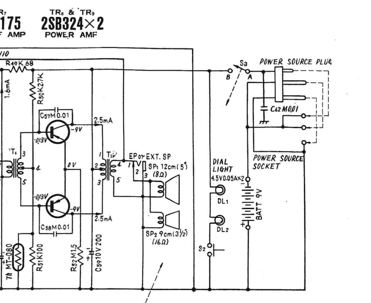
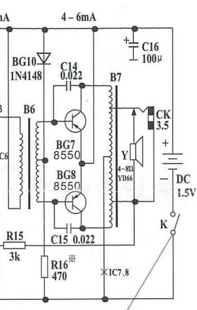
TODO - better (simplified) schematics, model (figure out appropriate inductor + resistor values for) input and output transformers
Relevant datasheets: 2SB324, SS8550
- For each stage, determine: (i) the gain; (ii) the output voltage swing; (iii) the output impedance; (iv) the efficiency?
- What class of amplifier are these?
- What is the purpose of the collector-base capacitors?
- The thermistor (top design) and the diode (bottom design) are both solutions to the same design problem. What is that problem and how do the two circuits solve it?
- Identify the main differences between the two stages and discuss the design choices behind them.
Solutions:
- TODO
- The transformer balun output might throw you off, and this isn’t the totem pole configuration, but assuming the base bias voltage is set accurately, each transistor conducts for 180 degrees of an input sinusoid’s cycle (upper and lower transistors for the positive and negative swings respectively). These stages are therefore class B.
- TODO – something something Miller effect?
- The design problem is that the base-emitter voltage drop changes with temperature (roughly 2 mV per degree Celsius), so a constant bias voltage with respect to temperature will introduce crossover distortion or excessive conduction when the temperature changes. The latter is especially worrisome since it can lead to thermal runaway: transistor conducts more current, causing it to heat up, causing the base-emitter voltage to decrease, causing it to conduct more current, and so on until it burns out. The thermistor obviously is chosen so that the base bias voltage tracks temperature appropriately. The forward voltage in the diode in the bottom circuit has a similar dependency on temperature to the transistor, again resulting in the base bias voltage appropriately tracking temperature.
- TODO
How can you tell if your system is being supplied with sufficient voltage? I had some really silly ideas when we were working on a uni design project. Main problem is bootstrap – how can you derive a reference voltage if you might not have enough voltage to get it? But this seems like basically a solved problem – see TI app note “Nano-Power Battery Monitoring in Personal Electronics”.
I recently bought a DIY AM radio kit as a gift for my sister. The accompanying instruction manual and directions turned out to be in Chinese, but fortunately the type, value and positioning of the components can be determined from the diagrams.
TODO: Does our 3106 decoupling circuit work? Why didn’t we get 2 V at the button site? And other questions… (postmortem)
(2024-05-01) Appendix J of The Art of Electronics (3rd ed.) uses the following RC circuit as part of a tutorial on SPICE analysis:
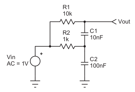
This circuit exhibits a voltage gain of 1.14 for an input signal of 1.1 kHz and has a gain greater than unity for frequencies from 100 Hz to around 2 kHz. I suppose this works out if you do your standard circuit analysis, but I’m trying to spot the intuitive reasoning. It is a second-order filter, so weird resonances aren’t out of the question.
(2024-05-03) Alright, I played around with some SPICE simulations and thought
about it some more. Right off the bat we figure we have two RC filters (1 kOhm
to 100 nF and 10 kOhm to 10 nF) which both have the same cutoff frequency of
1/(2*pi*R*C) = 1.59 kHz. Let’s make the assumption that the top RC branch
doesn’t significantly load the 1 kOhm resistor at the frequencies we’re looking
at (< 5 kHz) – its impedance ranges from infinity at DC (capacitor is open
circuit) to an absolute value of 22.4 kOhm at 5 kHz, so this turns out to be
a pretty safe bet. So if we take our output at the top of the 100 nF capacitor
we have a straightforward low-pass filter which gives us about 60 to 80% of our
signal around 1 to 3 kHz (very roughly).
Now say we have around 0.8 VAC (phase shifted by 30? 60? degrees) here at 1.1 kHz. To find the output voltage at the actual output we can use a hacky sort of superposition (relying on our loading assumption from before). (Warning: The following discussion uses very motivated reasoning because we already know the answer is “modest gain of 1.14”.) The top RC branch would put 0.8 VAC at the output if we grounded the top of the 100 nF capacitor. If we grounded the 1 VAC input then we have a high-pass filter (with cutoff frequency 1.59 kHz) from the point of view of the 0.8 VAC at the top of our 100 nF capacitor. At 1.1 kHz this is maybe going to result in 65% of the signal showing at the output, so around 0.5 VAC. Even with the phase shifts the magnitude of our output signal very slightly clears 1 VAC.
TL;DR: Low-pass filter a signal. High-pass filter the resulting signal (with the same cutoff frequency). Mix these to get a slight resonance near the cutoff frequency. This is more or less what the RC circuit above does.
Many “radio (or audio) for beginners” notes and textbooks talk about the frequency domain, or the idea that a time-varying signal can “contain different frequencies”, as though it’s self-evident. (TODO: include examples.) I didn’t understand what was meant by this until I took my second-year foundational EE course, which is a shame, because I could have understood it earlier if I’d taken the initiative to figure it out and find proper resources on the topic. Anyway, here is an outline of what the deal is:
- Periodic time-varying signals or functions (i.e. time-varying signals that
repeat themselves with some period T) can be expressed as an infinite sum of
sinusoids that have frequencies that are integer multiples of 1/T (the
“fundamental frequency”). The sum of sinusoids is known as the Fourier
series of the periodic function.
- I don’t think this is obvious to people who don’t spend a lot of time around periodic functions. What’s so special about sine waves? (It may be due to the fact that they are the most obvious and simple solutions to the wave equation…?)
- A square wave, for example, is clearly not a sine wave. But it turns out it can be approximated increasingly well by adding sine waves that are odd multiples of the fundamental frequency, scaled appropriately. In this sense, a square wave “contains” certain frequencies – a 10 kHz square waves “contains” a 10kHz sine wave, a 30 kHz sine wave, a 50 kHz sine wave, and so on. Any 10 kHz signal will “contain” frequencies at 10, 20, 30, 40, 50 etc. kHz; the amplitude and phase of these frequency components is what determines the actual shape of the signal. Or the shape of the signal determines the amplitude and phase of the signal’s frequency components, depending on how you look at it.
- It also turns out that you can kind of get a Fourier series for non-periodic signals and functions by treating the signal as periodic with a really long period (taking the limit as the period goes to infinity). This gets you a continuous function of frequency as an output. This operation is known as the Fourier transform. The input is a time-varying signal (your signal “in the time domain”) and the output is a function of frequency (your signal “in the frequency domain”).
- In this sense, now non-periodic signals (e.g. microphone inputs, speaker
outputs, sensor readouts, oscilloscope inputs) can be said to contain
different frequencies in different amounts even as they change over time.
- We’re still loosely talking about sums of sinusoids here – a signal can be reconstructed from its representation in the frequency domain by adding a bunch of sinusoids at the appropriate frequencies, we just aren’t restricted to these frequencies being harmonics of some fundamental frequency anymore. We use the grown-up tools of complex numbers instead of plain sine and cosine functions when we reach this step, though; it makes the mathematics easier.
- This is useful because a lot of things to do with signals are functions of frequency. For example, a network of passive components (or a linear network in general) can be characterised by a “transfer function”, from which you can obtain a “magnitude response” and a “phase response”, which are functions of input frequency. This can tell you by how much a sinusoid of some frequency is scaled and phase-shifted by the network, which, thanks to the Fourier transform, can tell you what the output of the network will be for any input signal. (Express the input signal as the sum of complex sinusoids, take the transfer function, and add the resulting complex sinusoids.)
This section would be much enhanced by some frequency spectrum plots. Oh well.
Pop Quiz SH-4RK-1 (STRAIGHTFORWARD BUT TEDIOUS): A classic Schmitt trigger oscillator is illustrated below. Derive the output oscillation in the time domain and determine (the first few values of) its Fourier series.
MISSING, TODO
Test Your Analog Design IQ: Written by the legendary Jim Williams. Attempting these questions made me feel rather stupid. I still don’t have a very good understanding of analog circuits, which I’m looking to rectify.
Question 3 of the analog design IQ test above represents a common 10x scope probe connected to a scope. Despite having been introduced to probe calibration before I did not spot this. I instead went about deriving the transfer function of the network and the magnitude response:
R_1 = 9 MOhm, R_2 = 1 MOhm, C_1 = 4 to 20 pF, C_2 = 77 pF
H(s) = (1 + s * R_2 * C_2)/((1 + R_1/R_2) + s * R_1 (C_1 + C_2))
|H(jw)| = sqrt(1 + T_2^2 * w^2)/(10 * sqrt(1 + (T_1/10)^2 * w^2)
where T_1 = R_1 * (C_1 + C_2) = 729 to 873 us and T_2 = R_2 * C_2 = 77 us.
Looking at the transfer function and magnitude response we see that the network
seems to attenuate DC and high frequency by a factor of 10 (20 dB). We can
guess that C_1 is supposed to be tuned to 8.555 pF to get a 20 dB attenuator
with a flat frequency response. And, had I actually thought about it, I might
have made the connection to an oscilloscope probe.
For reference, the following are extracts from a document on probe calibration, which my working mostly duplicates:
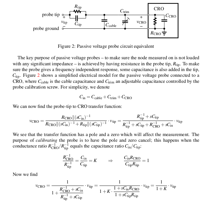
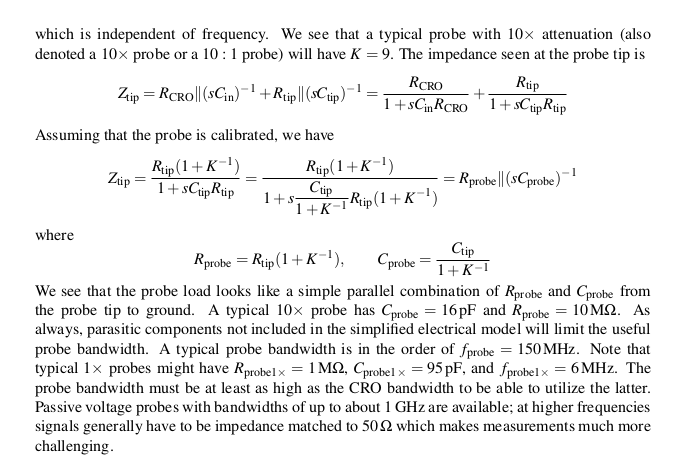
Pop Quiz AN47A-II (TRIVIAL): The following are CRO captures of a 500 Hz square wave as measured by probes compensated correctly and incorrectly. Derive the shapes of the over-compensated and under-compensated waveforms from first principles using the probe model outlined above with the probe capacitance set to either extreme (4 pF or 20 pF). Convince yourself that “over-compensated” here means “too much probe capacitance” instead of “not enough”.

TODO: solutions